Main PCB Assembly Manual
This manual will help with the project Quiver PT3 Main PCB assembly process.
Note: This is not a final version of this document. As of this time (June 2025) this PCB is not tested yet and not fully assembled. The given instructions will give a general guide on the assembly process. Assembly should only be carried out by an experienced worker with experience in SMD soldering and the appropriate equipment. If you need this PCB fully assembled please contact: julius@arrowair.com
This PCB can be ordered fully assembled from the respective PCB manufacturer (e.g. JLCPCB). There are several parts that are normally not in stock at the PCB manufacturer and need to be sourced from one of the large electronic component distributors by the PCB manufacturer. This means that the production time for a finished PCB is around 3 weeks.
The manual soldering of the circuit board can be done with the help of this interactive BOM which is stored in the respective github folder of this PCB:
Interactive BOM
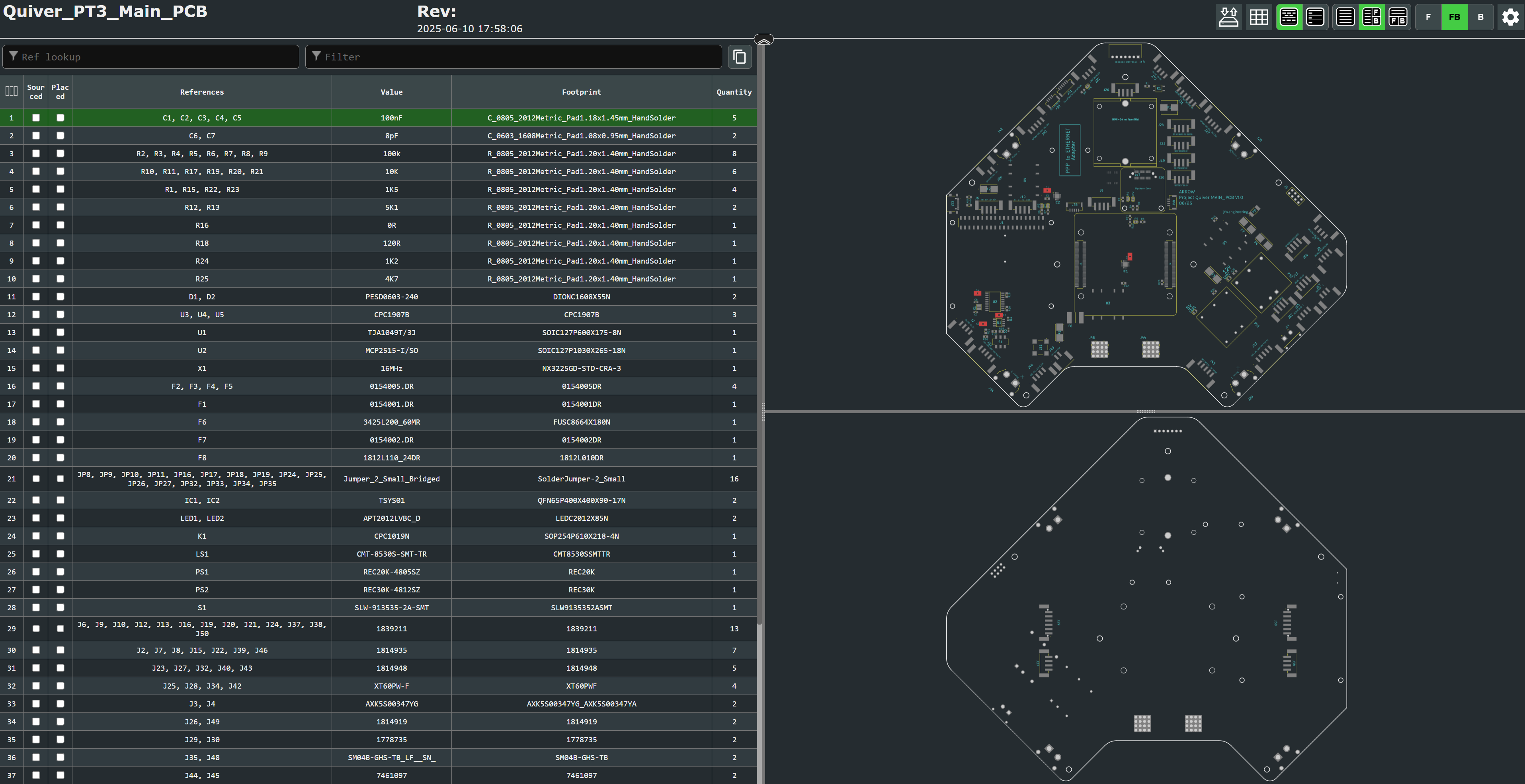
This is an HTML file that opens in the browser. On the left side is the parts list and on the right side are the views for the front and back of the circuit board. It will help to put the components in the right place.
It is essential to use a pcb stencil to place the solder paste in the right places. A reflow oven or a hot air blower (temperature and airflow controllable) should be used for the soldering process.
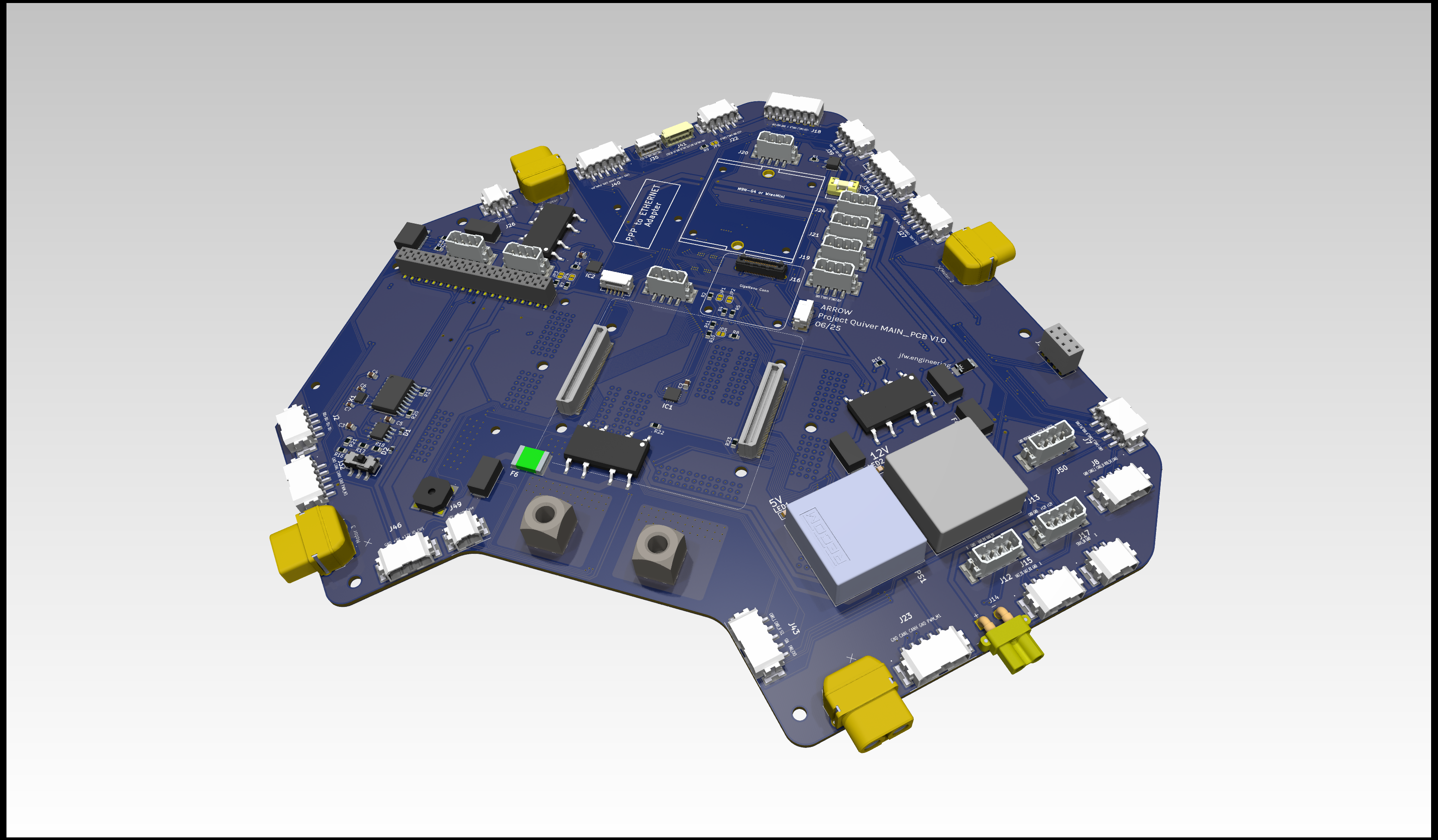
View on the top side of this PCB (this side contains all connections, except the connectors for the side attachment interfaces):
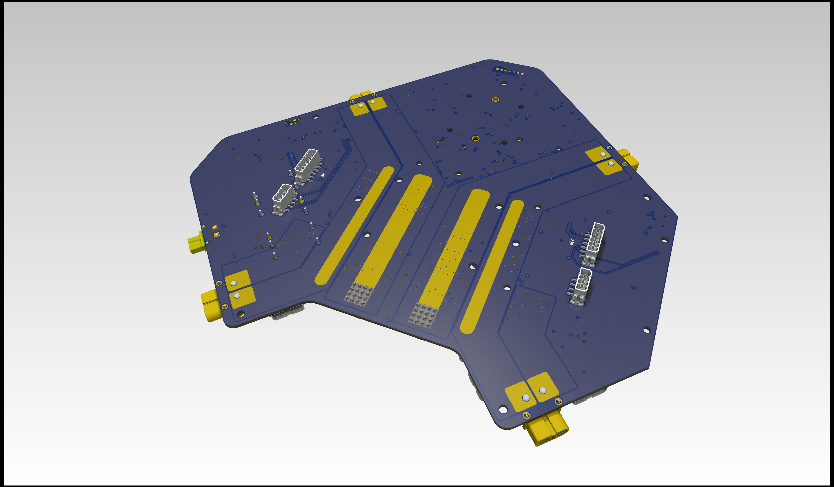
View on the bottom side of this PCB (this side contains the connectors for the side attachment interfaces):
Additional Steps
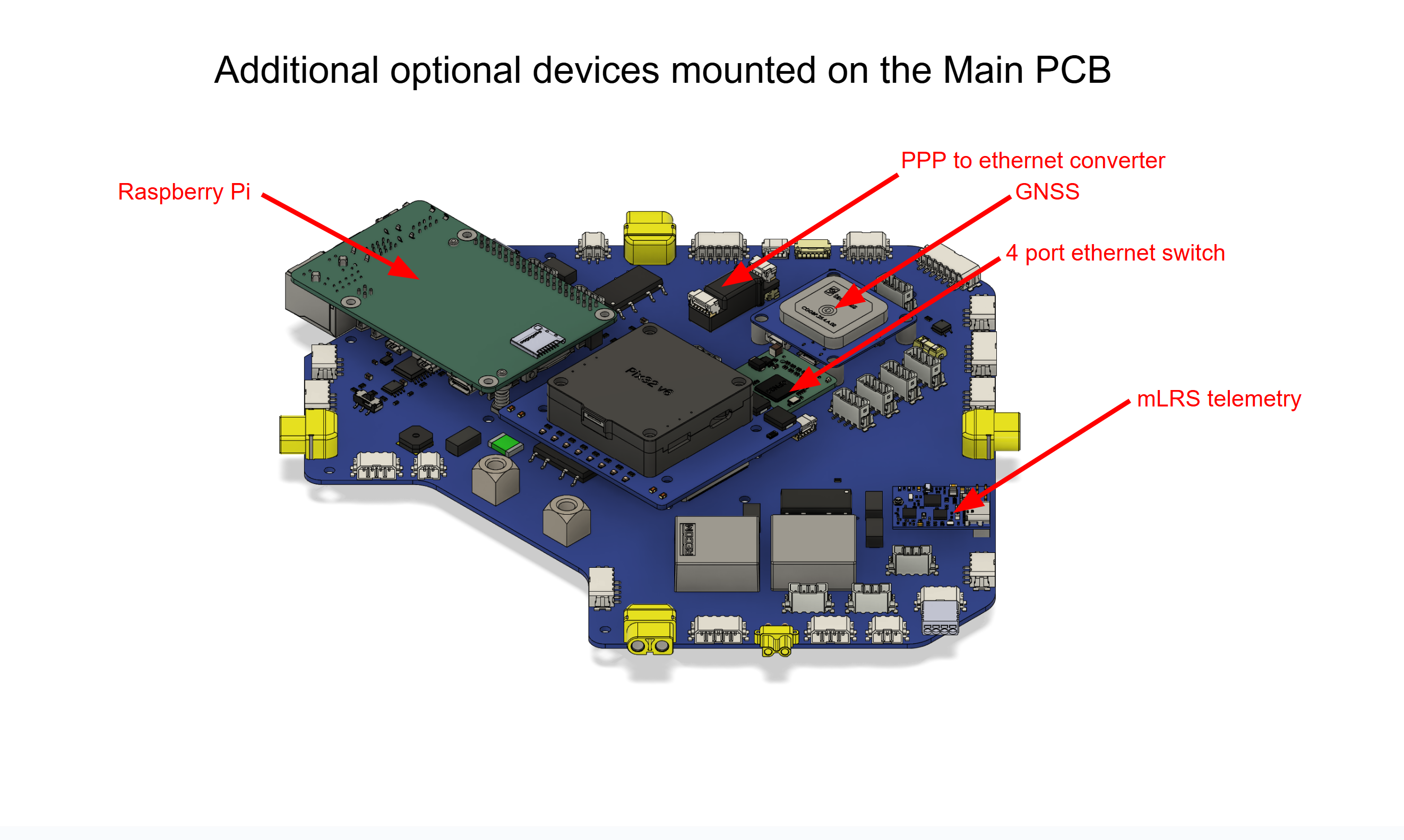
The main pcb has designated mounting positions for additional devices apart from the flight controller, which is placed in the center:
- A Raspberry Pi 5
- PPP to ethernet converter
- GNSS
- 4 port ethernet switch
- mLRS telemetry module
These additional devices are not necessary to ensure the basic function of the board.